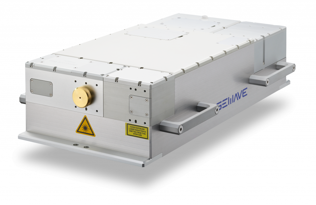
Ultrashort Pulse Lasers
Discover our ultrashort pulsed lasers of the PX and FX series.
PX Series
The PX series consists of ps-oscillator/amplifier systems based on InnoSlab technology:
- Beam quality: M² < 1.2
- Pulse energy: up to 2000 µJ
- Typical pulse duration: 12 ps
- Peak power: up to 170 MW
- Pulse repetition rate: up to 100 MHz
- Average power: up to 600 W
- Wave length: 1064, 532, 355, 266 nm

FX Series
The FX series consists of fs-oscillator/amplifier systems based on InnoSlab technology:
- Beam quality: M² < 1.2
- Pulse energy: up to 3000 µJ
- Pulse width typ.: 200 fs – 2000 fs
- Peak power: up to 1.5 GW
- Pulse repetition rate: up to 100 MHz
- Average power: up to 600 W
- Wave length: 1030, 515, 343, 258 nm

Ultrashort Pulse Lasers
Precise and material-saving
Our ultrashort-pulsed lasers are diode-pumped mode-locked solid-state oscillators and amplifiers based on the unique InnoSlab laser technology. Through an optimal combination of crystal shape, cooling, and resonator design, the ultra-short-pulse lasers of the PX and FX series offer numerous advantages:
- Compact design
- High efficiency and high gain factor
- High beam quality
- Scalable
- Beam quality: M² < 1.2
- Pulse energy: up to 3000 μJ
- Pulse duration: down to 300 fs
- Peak power: up to 3 GW
- Pulse repetition rate: up to GHz
- Average power: up to 600 W
- Wave length: IR, VIS, UV, DUV
- AI-ready

Applications
PX-Series
Lasers from the PX series can be used in a variety of applications. For example, in the following areas:
- Photovoltaics, such as scribing, drilling, ablation of conductive or dielectric layers in thin-film solar cells and crystalline silicon solar cells
- Printing industry, such as engraving printing rolls
- Electronics industry, such as drilling and cutting circuit boards
- Toolmaking and mechanical engineering, such as rapid 3D prototyping through ablation
FX-Series
Lasers from the FX series can be used in a variety of applications. For example, in the following areas:
- Photovoltaics, such as scribing, drilling, ablation of conductive or dielectric layers in thin-film solar cells and crystalline silicon solar cells
- Printing industry, such as engraving printing rolls
- Electronics industry, such as drilling and cutting circuit boards
- Toolmaking and mechanical engineering, such as rapid 3D prototyping through ablation